
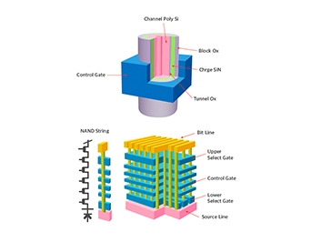
Due to the miniaturization of NAND flash memory processes, there has been a transition from Floating Gate to Charge Trap technology at nodes below 20nm. Consequently, the introduction of 3D structures is required for manufacturing NAND flash memory below 10nm.
These 3D stacked structures have a very high aspect ratio for holes, necessitating precise thickness control using ALD (Atomic Layer Deposition) equipment. As a result, low-temperature process SiO2 and SiN are required as high-quality materials for Blocking Oxide or Tunneling Oxide. The precursor used to form these oxide (SiO2) and nitride (SiN) films is HCDS (Hexachlorodisilane). The demand for this product is steadily increasing as semiconductor processes become more refined.
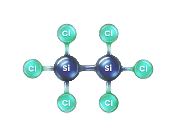
A material used as insulating films in semiconductor DRAM and NAND Flash memory production process)
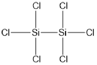
| Chemical name | Hexachlorodisilane |
|---|---|
| Cas No. | 13465-77-5 |
| Molecular formula | Si2Cl6 |
| Molar Weight | 268.88 g/mol |
| Physical State / Color | Colorless liquid |
| Boiling point | 144 ℃ |
| Vapor pressure | 40℃ / 12 Torr |
| Water reactivity | Violently reacts |